Samsung, SK hynix’s southwest fab plan faces talent take a look at as engineers weigh life past Seoul
When the top of SK hynix spoke in Seoul on Monday about Korea’s largest-ever semiconductor dedication, his first request to the federal government was not for cash, land or energy; it was for good colleges.
Without them, the chief government Kwak Noh-jung warned, sending younger engineers south might create “weekend couples,” the Korean shorthand for households cut up by a distant job posting.
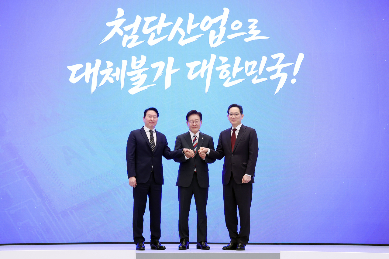
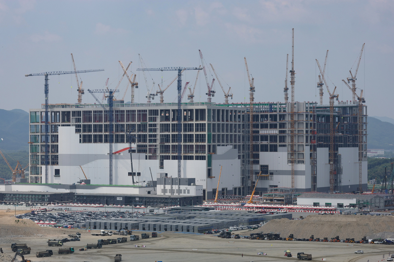
Samsung Electronics and SK hynix have dedicated a mixed 800 trillion received ($517 billion) to construct 4 reminiscence fabs in Jeonnam-Gwangju, a area some 300 kilometers southwest of Seoul, the federal government introduced Monday. Judging by what the executives requested for, one of many hardest constraints will not be capital; it’s whether or not expert employees will conform to reside there.
The doubt has a nickname. Job-seekers converse of a “southern recruitment limit” at Pyeongtaek, the Gyeonggi Province metropolis beneath which prime engineers have been reluctant to work. Pyeongtaek hosts Samsung’s largest chip complicated, the world’s largest single semiconductor web site.
The new fabs are sure for Honam, effectively beneath that mark.
Enough graduates, however not sufficient veterans
The argument over staffing the fabs runs alongside two tracks that always get blurred. The first is uncooked numbers, and that one is near settled.
Regional officers declare the world might end up a minimum of 2,000 chip-ready graduates a 12 months, cut up between universities and vocational colleges. Chonnam National University, the area’s flagship public college, graduates greater than 500 a 12 months from departments tied to chipmaking, spanning electronics, supplies, chemistry and physics. The Gwangju Institute of Science and Technology runs a program that admits 30 college students a 12 months and funnels them straight into Samsung below a guaranteed-hiring contract. The institute additionally has a separate design academy constructed with Britain’s Arm, the agency whose chip blueprints are inside a lot of the world’s smartphones, which goals to coach 1,400 designers over 5 years.
Half a dozen different native universities have added semiconductor majors of their very own, and the newly merged regional authorities has set a goal of coaching 100,000 employees throughout synthetic intelligence, vitality and chips.
“Local talent alone is enough to run these fabs,” Ryu Sang-wan, a professor on the Gwangju-Jeonnam Joint Semiconductor Research Institute at Chonnam National University, informed The Korea Herald. He famous that Amkor’s packaging plant in Gwangju “already employs about 4,500,” however admitted {that a} front-end fab, which handles the complicated early phases of chipmaking, “would need far more.”
Ryu defined that automation has thinned the operator ranks of a fab workforce and made engineers the majority of a contemporary plant, and people engineers are the graduates the area can provide.
Lee Min-jae, dean of GIST’s graduate college of semiconductor engineering, mentioned the southern restrict line exists solely “because the good jobs are all clustered in the capital region.” Honam has educated expert individuals for years, he mentioned, however the capital “absorbed all of them.” Building fabs within the south, in response to his logic, is the repair, not the gamble.
Fabs can transfer south. Expertise might not comply with
A graduate will not be the identical as an engineer who can run a line. New hires have by no means touched the gear, Ryu mentioned, and a modern fab’s machines are too pricey for any campus to repeat, in order that they should be “trained on the line, next to people who already know it.” Early on, that have has to return down from the capital area, he admitted.
The corporations’ deepest fear is that the few thousand grasp’s- and doctoral-level engineers who handle chip design and yield — the individuals who determine whether or not a line runs at a revenue or a loss — have confirmed hardest to maneuver south.
Hwang Cheol-sung, a supplies science professor at Seoul National University, informed native media that Korea’s edge comes from conserving analysis and manufacturing aspect by aspect, the place an engineer can take a look at an thought on the road and see the consequence the identical day. The most superior instruments are too pricey to duplicate in a separate lab, so researchers work on the reside manufacturing ground, an association that breaks the second the fab sits in Honam and the labs keep close to Seoul.
Pull the 2 aside, he warned, and “competitiveness is bound to fall sharply,” pointing to US rival Micron, its labs and fabs scattered throughout nations, because the cautionary case.
There is precedent at dwelling. When Samsung Display constructed a fancy in Asan, South Chungcheong Province, prime engineers reportedly balked at relocating. The repair then, analysts say, was cash and livability: sustained bonuses and facilities adequate to maintain individuals in place.
President Lee Jae Myung, who has staked his presidency on loosening Seoul’s grip on the nation’s wealth, mentioned the aim was “not just to build factories, but to make places where people want to live,” pledging funding to make the area even rival the capital.
What no coverage can rapidly change is the calculation within the engineers’ personal minds. One Samsung engineer, 5 years in, informed The Korea Herald he had simply purchased a house in Seoul to begin married life and was unsettled by discuss of a far posting.
“A plant moving,” he mentioned, “doesn’t automatically mean its people move with it.”
By Moon Joon-hyun ([email protected])