When the United States made the strategic resolution in 2020 to reinvest in home semiconductor manufacturing, it confronted an uncomfortable paradox baked into capitalism itself: How do you create the collaborative surroundings it would take to be a worldwide chief when the American {industry} is made from corporations structured as opponents?
This gradual conversion is coming collectively this yr in Silicon Valley — and Arizona State University is correct in the midst of it — in a facility designed from the bottom as much as make that form of collaboration not simply potential, however inevitable.
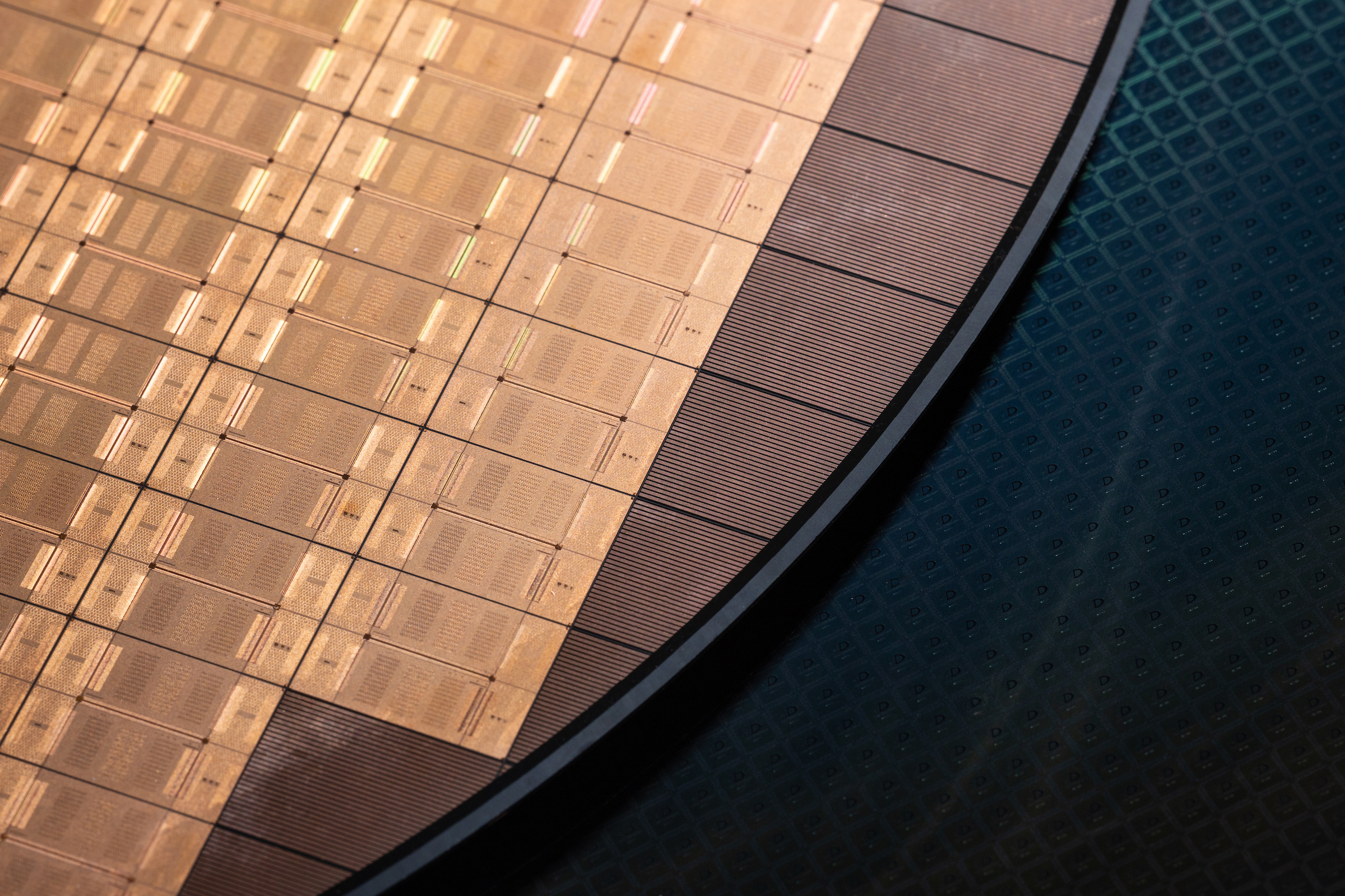
ASU has been named an inaugural university research partner at Applied Materials‘ new EPIC Center — brief for Equipment and Process Innovation and Commercialization — the largest-ever U.S. funding in superior semiconductor tools research and improvement.
Joining ASU as tutorial companions will likely be Rensselaer Polytechnic Institute and Stanford University in a facility that counts AMD, IBM, Intel, Micron, Nvidia, Samsung, TSMC and Western Digital amongst its {industry} contributors.
“With the largest engineering school in the country, ASU is driven by our commitment to be of service to industry and to create partnerships that accelerate defining breakthroughs for future semiconductor technology,” ASU President Michael Crow mentioned. “Being a part of a high-velocity, high-creativity environment with the brightest minds in the industry builds upon the work we do with Applied Materials in our shared Materials-to-Fab Center at ASU, creating a seamless network for driving semiconductor excellence in America.”
The EPIC Center introduces a structurally novel mannequin to the semiconductor {industry}: For the primary time, chipmakers can keep devoted house inside an tools provider’s facility, successfully extending their very own in-house pilot strains whereas gaining early entry to next-generation instruments and applied sciences — months and even years forward of when equal capabilities might in any other case attain their very own labs.
The middle is designed to compress the timeline from early-stage research to full-scale manufacturing by quicker studying cycles, higher accuracy and tighter collaboration throughout the complete innovation chain.
“The EPIC Center is designed to bring together the best minds from industry and academia in a high-velocity, manufacturing-relevant environment to dramatically accelerate the development and commercialization of next-generation semiconductor technologies that are foundational to AI computing,” mentioned Gary Dickerson, president and CEO of Applied Materials. “Welcoming ASU, RPI and Stanford as research partners at EPIC strengthens the U.S. lab-to-fab innovation pipeline and creates a powerful platform for developing future semiconductor talent.”
For ASU, the EPIC Center partnership builds instantly on an already deep relationship with Applied Materials. In October 2025, the 2 establishments collectively opened the $270 million Materials-to-Fab Center at ASU’s MacroTechnology Works facility in Tempe — a shared R&D and prototyping surroundings that brings industry-scale semiconductor manufacturing tools right into a collaborative university setting. The Materials-to-Fab Center already helps ASU research initiatives tied to the CHIPS and Science Act, together with the Southwest Advanced Prototyping Hub and the SHIELD USA superior packaging initiative.
“Being selected as one of three inaugural university partners at the EPIC Center reflects ASU’s rise to national prominence in semiconductor research and innovation,” said Sally Morton, executive vice president of ASU’s Knowledge Enterprise. “The largest U.S. semiconductor equipment manufacturer choosing to work with the top U.S. research universities is itself a statement. Our relationship with Applied Materials has strengthened through our collaboration in the Materials-to-Fab Center and our ability to deliver results. We expect industry partners to bring their hardest problems to this environment, and our researchers will be there to help solve them.”
Morton noted that this alignment between real-world challenges and academic inquiry is a critical element to advancing U.S. competitiveness. The mission is to accelerate the development of high volume manufacturing.
ASU brings to the partnership the largest engineering school in the United States, with approximately 33,000 students, along with deep expertise that spans the full microelectronics ecosystem — from front-end materials innovation through advanced packaging and large-scale manufacturing. The university has emerged as a key recipient of state, federal and private sector investment in microelectronics, and its SWAP Hub is part of the national Microelectronics Commons created through the CHIPS and Science Act.
“What makes the EPIC Center genuinely completely different and finally of nice worth is that it brings collectively the complete ecosystem in a single place — software producers, chipmakers, supplies suppliers and universities all working in shut proximity, with entry to essentially the most superior tools within the {industry},” mentioned Jason Conrad, chief working officer of the SWAP Hub.
“Right now, getting access to the latest technologies and, more importantly, getting access to the actual problems customers are trying to solve — that’s extraordinarily difficult,” Conrad said. “The EPIC Center changes that. It puts our researchers at the table alongside the people who are going to define what the next generation of semiconductor technology looks like, and it allows us to accelerate in ways that simply aren’t possible when academia and industry operate in separate lanes.”
EPIC Center will change into operational later this yr.