The firm mentioned it has efficiently utilized Atomic Layer Etching (ALE) to manufacture and refine the quantum‑engineered constructions that underpin ULTRARAM gadgets. The work is being carried out at KAUST Core Labs using ALE know-how provided by Oxford Instruments.
The newest processing builds on greater than a decade of quantum system analysis undertaken at Lancaster University, with KAUST now offering superior fabrication capabilities. According to Quinas, the mix permits sub‑nanometre precision and extremely‑low‑injury processing, which is crucial for establishing the extremely managed quantum nicely heterostructures required by ULTRARAM.
ULTRARAM is designed to ship reminiscence efficiency akin to DRAM whereas retaining information with out energy, a mix that might considerably enhance power effectivity and system‑degree efficiency. Achieving this depends upon exact management of interfaces and layer thicknesses inside advanced III–V semiconductor supplies, making atomic‑scale fabrication strategies notably nicely suited to the know-how.
“Atomic‑scale control of our quantum well structures is fundamental to ULTRARAM,” mentioned James Ashforth‑Pook, chief government and co‑founding father of Quinas Technology. “Working with KAUST Core Labs and leveraging Oxford Instruments’ Atomic Layer Etching technology gives us access to one of the world’s most advanced and credible environments for low‑damage semiconductor R&D.”
KAUST Core Labs is recognised for its capabilities in nanofabrication, plasma processing and compound semiconductor analysis, supporting each tutorial programmes and industrial know-how growth.
“KAUST Core Labs support cutting‑edge semiconductor research through advanced nanofabrication facilities and atomic‑scale processing tools designed for low‑damage device development,” mentioned Dr Kenneth Kennedy, director of the KAUST Nanofabrication Core Lab.
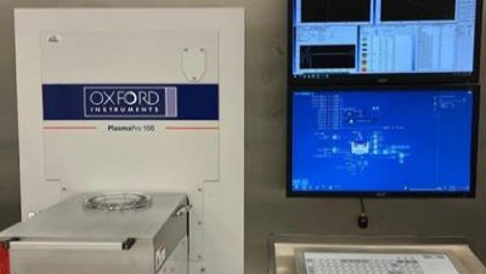
Oxford Instruments mentioned the collaboration highlights the rising adoption of ALE strategies in superior system analysis. “Atomic Layer Etching enables precise, low‑damage fabrication of nanoscale device features and is increasingly used in advanced semiconductor research and production environments worldwide,” mentioned Harriet van der Vliet, head of strategic R&D markets at Oxford Instruments Plasma Technology. She added that KAUST operates a collection of ALE and Atomic Layer Deposition programs, together with the PlasmaProfessional ASP.
Quinas mentioned the work at KAUST displays its broader worldwide analysis technique and marks a step in the direction of prototype demonstrations of ULTRARAM. The firm mentioned it’s positioning the know-how for future engagement with industrial companions, semiconductor foundries and potential strategic traders as growth progresses.