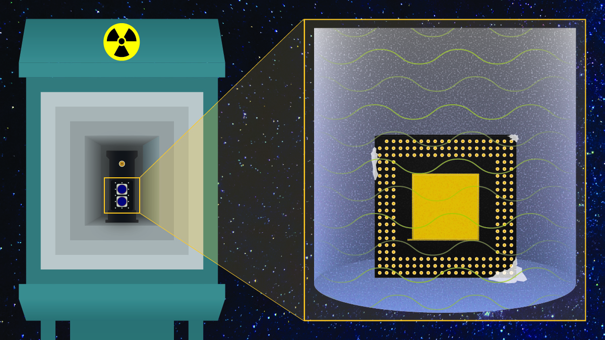
Imagine a microchip on a satellite tv for pc in low Earth orbit. Temperatures swing from minus 85 levels Fahrenheit to over 250 F. In one 12 months, it is bombarded with over 100 instances the radiation dose the common individual experiences naturally on Earth. And if it wants new elements, nicely, it should wait a decade or so.
At Arizona State University, researchers and college students within the Extreme Environments Lab check semiconductor applied sciences underneath a number of the harshest situations. The lab serves the Southwest Advanced Prototyping, or SWAP, Hub, supporting authorities and trade companions in designing applied sciences which might be dependable in demanding settings.
This functionality is vital throughout a big selection of purposes — from house stations and missile protection methods to geothermal power and oil exploration tools deep underground. It additionally helps radiation remedy, nuclear power methods and superior scientific instruments equivalent to quantum computer systems.
ASU’s SWAP Hub is a part of the Department of Defense’s Microelectronics Commons. It is the one regional hub with complete infrastructure for testing electronics in extreme temperature and radiation environments. By involving college students at each stage, the lab helps them acquire in-demand abilities and hands-on expertise that translate on to profession alternatives.
What occurs throughout extreme setting testing?
“Imagine equipment in space. You can’t replace parts easily. Things need to last for 10 to 20 years up there under extreme conditions,” says Hugh Barnaby, who leads extreme setting reliability efforts within the SWAP Hub.
That actuality underscores why builders wish to guarantee their applied sciences carry out as supposed.
“There are different classifications for specifying whether these applications can work in certain environments. For us in SWAP Hub, we are working with the extreme environment specifications, which is way outside of the bounds of even military specifications in terms of temperature operation,” says Barnaby, who is additionally a professor within the School of Electrical, Computer and Energy Engineering.
Barnaby leads the Extreme Environment Lab staff, which checks semiconductor parts with particular tools from the ASU Eyring Materials Center, a part of ASU’s Core Facilities, and SWAP Hub accomplice amenities. The staff evaluates strain, humidity, mechanical shock and excessive temperature, however locations a heavy give attention to radiation publicity and extreme chilly, each collectively and individually. The researchers can even check know-how throughout or after publicity.
Being capable of check completely different types of radiation permits the lab to serve many consumers. Galactic cosmic rays in house, for instance, are very completely different from proton radiation utilized in most cancers remedy. The lab ensures that vital know-how will work within the particular setting the place folks will use it.
The lab additionally performs modeling and evaluation to foretell efficiency, discover issues early and information design enhancements.
Student-led options
PhD scholar Jereme Neuendank has embraced inventive drawback fixing within the lab. One problem concerned testing units underneath extreme chilly and radiation on the identical time.
Normally there is one machine to check extreme chilly and one other to check radiation. Neuendank helped develop a cryogenic system sufficiently small to suit contained in the lab’s radiation chamber — the Rigel DSTAT.
“The main reason we wanted to do that is because in a space environment, a microchip will usually be at a very cold temperature when it’s getting exposed to radiation. So to get a more accurate scope of how these devices are going to perform, we wanted to simulate those environments as closely as we could. Being able to irradiate at cryotemperatures was a big breakthrough that we came up with,” says Neuendank, who is within the School of Electrical, Computing and Energy Engineering.
He additionally helped develop a distant testing system in order that experiments — some lasting as much as 10 hours — might run while not having a researcher bodily current within the lab.
During a summer time internship with Sandia National Laboratories, Neuendank used a comparable answer to streamline a setup that had pressured researchers to modify between two computer systems. The lab nonetheless makes use of his system to this present day, he says.
“I like a good challenge. The Rigel DSTAT certainly didn’t exist before, so it all had to be created,” says Neuendank, who hopes to work in trade after commencement. “It’s a good learning experience to get familiar with building those types of testing systems and trying to build them in such a way where they’re loosely applicable to a wide variety of different testing environments.”
Tyler Kirby, additionally a PhD scholar within the School of Electrical, Computing and Energy Engineering, focuses on modeling and evaluation. Using superior laptop simulation instruments, he builds digital units and research how radiation impacts them. Much of his work is a part of a year-round distant internship with Sandia.
“It was always hard for me to pick one area of interest,” says Kirby, who hopes to do research-based work in a nationwide lab after graduating. “I really like how this combines so many different areas, like materials science, electrical engineering, physics, radiation, chemistry.”
Helping the US authorities and trade alike
As a part of the SWAP Hub, Barnaby’s lab helps know-how builders rapidly meet U.S. protection and trade wants for applied sciences that carry out in extreme environments.
The SWAP Hub connects over 200 members — chip producers, protection companies, nationwide labs, startups and different organizations — offering entry to shared amenities, tools and experience to strengthen U.S. technological management.
Partners flip to the lab for assist fixing advanced issues, figuring out design flaws and validating efficiency underneath extreme situations. The staff usually works with semiconductor parts equivalent to circuits, transistors and capacitors by way of each bodily testing and modeling.
For instance, the lab is collaborating with Kyocera to check how its capacitors reply to radiation and with Microchip Technology to judge radiation results on energy transistors.
The outcomes assist companions refine merchandise and processes, guaranteeing vital applied sciences carry out when it issues most.
“Our group walks along with them and supports all of the testing that they need to be confident that their product is good for extreme environments,” Barnaby says.
Why this research issues
Research is the invisible hand that powers America’s progress. It unlocks discoveries and creates alternative. It develops new applied sciences and new methods of doing issues.
Learn extra about ASU discoveries which might be contributing to altering the world and making America the world’s main financial energy at researchmatters.asu.edu.