Scientists have lastly packed a laboratory-class ultrafast laser onto a tiny photonic chip.
Ultrafast lasers generate bursts of sunshine that final solely a few hundred femtoseconds, each simply a quadrillionth of a second lengthy. These extraordinarily quick pulses are utilized in a wide selection of applied sciences, together with precision manufacturing, eye surgical procedure, and optical frequency combs, the Nobel Prize-winning innovation that powers the world’s most correct optical atomic clocks.
Despite their significance, ultrafast lasers have typically remained massive, pricey methods that occupy total optical tables in analysis laboratories. After greater than twenty years of labor by scientists around the globe, shrinking these units onto a photonic chip has remained an elusive objective.
Now researchers led by Professor Tobias J. Kippenberg at EPFL have achieved that milestone. Writing in Nature, the crew studies the primary built-in ultrafast laser able to matching the efficiency of conventional tabletop femtosecond lasers, producing pulses as quick as 147 femtoseconds with energies reaching 1.05 nanojoules.

Bringing Ultrafast Lasers to Photonic Chips
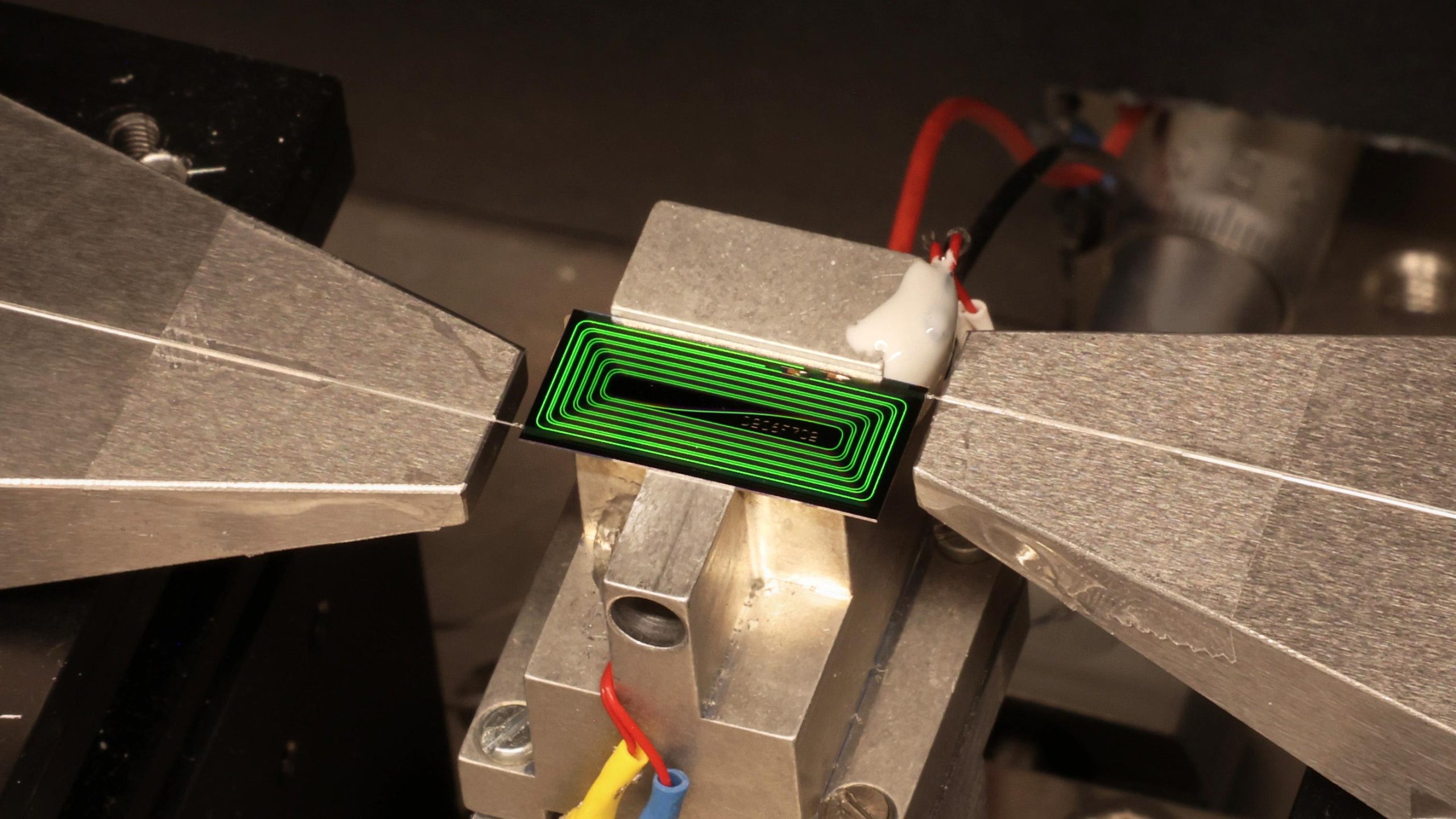
Photonic chips manipulate mild utilizing microscopic buildings known as waveguides which can be patterned onto a wafer. In some ways, they operate like digital chips, besides they direct mild fairly than electrical currents. These chips are already extensively utilized in telecommunications and have helped shrink many optical applied sciences that when required a lot bigger tools.
“For more than twenty years, a high-pulse-energy femtosecond laser on chip was widely regarded as a holy grail of integrated photonics,” says Kippenberg. “Our result shows that it is not only possible, but that it can be achieved with a surprisingly elegant architecture that the integrated-photonics community had overlooked.”
An Overlooked Laser Design
To attain this objective, the researchers adopted a little-used laser structure generally known as the Mamyshev oscillator.
Inside the laser cavity, a nonlinear waveguide is positioned between two optical filters, every of which passes a totally different portion of the sunshine spectrum. As a robust pulse travels by the waveguide, its spectrum broadens, permitting a few of that mild to move by each filters and proceed circulating throughout the cavity. Weaker mild doesn’t broaden sufficient and is filtered out.
“This design is especially attractive because it does not require any component that is difficult to make on this erbium-doped silicon nitride chip,” explains Zheru Qiu, a co-leading writer of the paper.
According to Qiu, the design presents one other main benefit. Photonic chips confine mild to extraordinarily small waveguides, which will increase nonlinear interactions between mild waves. In many standard laser designs, these interactions can destabilize the laser pulses. The Mamyshev oscillator, nevertheless, is way much less delicate to these results, making it significantly nicely suited to built-in photonic units.
Tiny Device, Major Potential
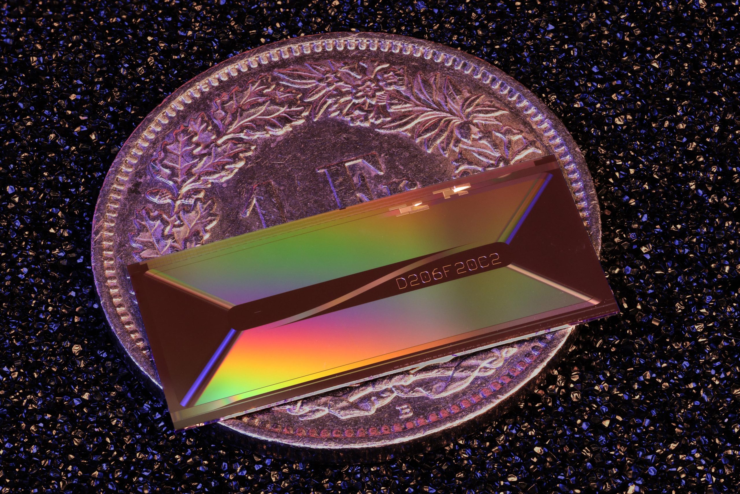
The laser cavity measures 42 centimeters in size, but it may be folded onto a chip occupying roughly the realm of a match head. That makes it dramatically smaller than standard fiber-based ultrafast laser methods.
Because photonic chips might be fabricated on the wafer degree utilizing manufacturing strategies just like these used for pc chips, greater than 1,000 laser cavities may doubtlessly be produced in a single batch. This functionality may considerably cut back prices whereas increasing entry to ultrafast laser expertise for sensing, spectroscopy, and precision measurement purposes.
“With kilowatt-level peak powers, the chip can drive demanding applications that have long depended on large, expensive laboratory lasers,” says Qiu.
The advance may finally result in compact and reasonably priced units for detecting environmental pollution, figuring out hidden materials defects, and performing medical diagnostics. It may assist pave the way in which for transportable optical atomic clocks that would help future communication and navigation applied sciences.
Reference: “High-pulse-energy integrated mode-locked laser using a Mamyshev oscillator” by Zheru Qiu, Xuan Yang, Xurong Li, Jianqi Hu, Zhongshu Liu, Yichi Zhang, Xinru Ji, Jiale Sun, Grigory Lihachev, Zihan Li, Ulrich Kentsch and Tobias J. Kippenberg, 3 June 2026, Nature.
DOI: 10.1038/s41586-026-10517-4
Other Contributors
- EPFL Institute of Electrical and Microengineering
- Helmholtz-Zentrum Dresden-Rossendorf (HZDR)
Never miss a breakthrough: Join the SciTechDaily newsletter.
Follow us on Google and Google News.