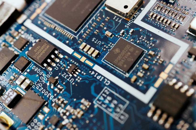
In a high-security laboratory in Shenzhen, China, scientists have developed a prototype machine able to producing superior semiconductor chips essential for applied sciences resembling synthetic intelligence and army functions, a objective that the U.S. has lengthy sought to forestall. This prototype, accomplished in early 2025 and presently within the testing section, occupies virtually a whole manufacturing facility flooring. It was assembled by a gaggle of engineers beforehand employed by ASML, a Dutch semiconductor firm, who reverse-engineered the acute ultraviolet lithography machines (EUVs) important for chip manufacturing.
EUV machines make the most of excessive ultraviolet mild to carve out infinitesimal circuits on silicon wafers—a capability that is still predominantly within the palms of Western firms. Despite being operational and efficiently producing excessive ultraviolet mild, the machine has but to provide functioning chips. ASML CEO Christophe Fouquet not too long ago steered that China may require “many, many years” to accumulate this know-how, however the existence of the prototype signifies that China’s timeline could also be considerably shorter than projected.
However, vital technical challenges persist, predominantly in attaining the precision present in Western optical methods. The availability of parts from older ASML machines within the secondary market enabled China to assemble its home prototype, with aspirations to provide working chips by 2028, though extra lifelike estimates recommend 2030. This continues to be forward of the last decade that many analysts had anticipated can be required for China to equal the West’s semiconductor capabilities.
The prototype’s growth is a end result of a six-year initiative aimed toward semiconductor self-sufficiency—a precedence of President Xi Jinping. While China’s semiconductor ambitions have been publicly acknowledged, the Shenzhen EUV venture has remained largely secretive. The venture is a part of a broader technique overseen by Ding Xuexiang, a detailed affiliate of Xi Jinping and head of the Communist Party’s Central Science and Technology Commission.
Huawei performs an important position in orchestrating this initiative, coordinating efforts amongst numerous firms and analysis institutes. The operation has been in comparison with the U.S. Manhattan Project, with the goal of attaining full self-sufficiency in superior chip manufacturing.
Historically, ASML stands as the only real enterprise to have perfected EUV know-how, with machines priced round $250 million which can be pivotal for creating state-of-the-art chips utilized by firms like Nvidia and AMD. ASML’s growth of EUV know-how spanned almost twenty years and concerned in depth funding earlier than its first industrial chips had been produced in 2019.
Since 2018, the U.S. has pressured the Netherlands to ban ASML from promoting EUV gear to China, and in 2022, the Biden administration broadened export controls to restrict China’s entry to cutting-edge semiconductor know-how. These controls goal not simply EUV methods but in addition older deep ultraviolet lithography machines, aimed toward preserving China at the very least one technology behind in chip growth. The U.S. State Department has acknowledged that enforcement of those export controls has been strengthened, working with worldwide companions to handle potential loopholes.
Chinese semiconductor growth has confronted hindrances on account of these export restrictions, impacting main gamers like Huawei. Sources emphasize the confidentiality surrounding the Shenzhen venture, noting that members had been instructed to make use of false identities to keep up operational secrecy. Recruited engineers included former ASML workers who possess essential technical experience, permitting the workforce to efficiently reverse-engineer the know-how.
Recruitment efforts for engineers proficient in semiconductor know-how have been aggressive since 2019, with affords of considerable signing bonuses and incentives resembling home-buying help. Notable recruits embody Lin Nan, ASML’s former head of sunshine supply know-how, who has made strides in patent developments associated to EUV mild sources.
While ASML claims to safeguard its commerce secrets and techniques rigorously, it faces challenges on account of European privateness legal guidelines, making it tough to watch former workers. The Dutch intelligence group has warned that China has utilized in depth espionage operations to accumulate superior data and know-how from Western nations, additional illustrating the aggressive panorama. Even with authorized frameworks in place, enforcement of confidentiality agreements throughout worldwide borders stays complicated.
Furthermore, the recruitment of personnel working in superior know-how sectors continues to attract scrutiny, as people have been reportedly incentivized with extra advantages, together with twin citizenship preparations that enable some to keep up affiliations with a number of nationalities regardless of official restrictions.
As the Chinese authorities pushes in the direction of its semiconductor self-sufficiency targets, it’s evident that their efforts to slender the technological hole with the West are intensifying. Despite the hurdles forward, the Shenzhen venture represents a major step ahead in China’s quest to dominate semiconductor manufacturing, with implications not just for the worldwide know-how panorama but in addition geopolitically relating to provide chains and technological dependencies.
INSIDE CHINA’S EUV FAB
ASML’s newest EUV methods measure the scale of a faculty bus and weigh 180 tons, with China’s prototype considerably bigger to boost energy, although it stays crude in comparison with ASML’s machines. The Chinese mannequin is hampered by challenges in buying optical methods from Carl Zeiss AG, a key provider for ASML. China’s main analysis institutes, particularly the Changchun Institute of Optics, Fine Mechanics and Physics (CIOMP), are essential in creating home alternate options. CIOMP made strides in integrating extreme-ultraviolet mild into the optical system projected to be operational by early 2025, regardless of needing substantial enhancements.
To appeal to expertise, CIOMP marketed “uncapped” salaries for PhD lithography researchers and grants totaling 4 million yuan ($560,000) together with private subsidies of 1 million yuan ($140,000). Analyst Jeff Koch from SemiAnalysis famous that if China achieves a dependable, highly effective mild supply with minimal contamination, it might signify substantial progress. China’s benefit lies in not ranging from scratch since industrial EUV already exists.
To procure needed parts, China is utilizing salvaged components from older ASML machines and sourcing from ASML suppliers by way of secondhand markets, usually using middleman firms to obscure the last word purchaser. Export-restricted parts from Japan’s Nikon and Canon are additionally built-in into the prototype, although Canon indicated no consciousness of such experiences. Recent auctions usually listed older semiconductor fabrication gear, together with ASML lithography gear, indicating a market presence for such components.
China has a devoted workforce of round 100 latest graduates engaged in reverse-engineering each EUV and DUV lithography machine parts. Each workspace is monitored by way of particular person cameras to doc the disassembly and reassembly course of crucial for developments in lithography. Workers who efficiently reassemble parts obtain bonuses as an incentive.
Huawei performs a major position in the whole provide chain, from chip design and fabrication to last product integration, carefully monitored by CEO Ren Zhengfei, who briefs high-ranking officers on progress. Employees at Huawei usually work in isolation inside semiconductor groups, sleeping on-site throughout workweeks, with strict communication limits imposed to keep up venture confidentiality, emphasizing the excessive safety surrounding their work on semiconductor developments.
With data from Reuters