Researchers from KAUST, TU Delft, and LMU Munich have improved the efficiency of monolithic perovskite-silicon tandem solar cells by modifying the bodily construction on the entrance of the underside heterojunction solar cell.
A analysis crew from Delft University of Technology (TU Delft), King Abdullah University of Science and Technology (KAUST), and Ludwig-Maximilians-Universität München (LMU Munich) has proven that controlling nanoscale floor roughness on the recombination layer in perovskite-silicon tandem solar cells can enhance efficiency.
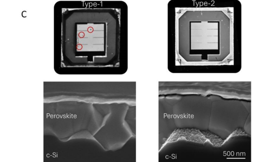
Noting that the affect of the crystalline silicon (c‑Si) backside cell nanoscale floor roughness has acquired far much less consideration than perovskite optimization, the researchers investigated the results of floor modification of the silicon heterojunction (SHJ) backside cell to know the affect of the floor nanoroughness on tandem gadget efficiency.
“The key novelty of our study lies in demonstrating that the nanoroughness of the recombination junction can be deliberately engineered to significantly improve the performance of perovskite-silicon tandem solar cells,” Erkan Yadin, co-corresponding writer of the analysis, instructed pv magazine. “By systematically tuning the surface morphology at the nanoscale, we improved electrical contact quality and reduced recombination losses, which led to reproducible and higher efficiency results.”
“This provides a new design parameter that is compatible with existing silicon heterojunction technology,” added Yadin.
The crew’s tandem optimization method is differentiated from these that concentrate on supplies composition, interface passivation, or optical administration. “Our design strategy complements these efforts by addressing the physical structure of the recombination junction itself. Importantly, this approach does not require new materials or complex processing steps, making it highly synergistic with established silicon heterojunction and perovskite fabrication routes,” mentioned Yadin, including that it provides a “scalable and manufacturable pathway to further boost tandem performance.”
In the research, the crew investigated variations in thickness and plasma remedies of n-type (n) hydrogenated nanocrystalline silicon ((n)nc-Si:H) skinny movies. “We tailored the (n)nc-Si:H nanoroughness by (i) adjusting the thickness of the (n)nc‑Si:H layers and (ii) applying plasma treatment using a hydrogen (H2) and carbon dioxide (CO2) gas mixture for varying durations prior to (n)nc‑Si:H layer depositions,” it mentioned.
In testing, each strategies have been discovered to boost the conductivity and crystallinity of (n)nc-Si:H layers and improve the floor nanoroughness, with plasma therapy enabling the environment friendly realization of distinct nanoroughness in skinny (n)nc-Si:H (15-nm-thick) layers.
The systematic variation of the plasma therapy period enabled managed variation of the floor nanoroughness of textured c-Si backside cells, selling improved tin-doped indium oxide (ITO)/gap transport layer (HTL)/perovskite interfaces, which enhanced tandem gadget efficiency, in accordance with the analysis.
“Our results reveal that the surface nanoroughness imposed by (n)nc-Si:H layers influences the self-assembled monolayer (SAM) anchoring, leading to increased work function shifts and improved SAM/perovskite interface quality, thereby impacting the overall tandem device performance,” mentioned the researchers.
“Notably, tandem devices incorporating higher-nanoroughness bottom cells achieved increased fill factors, dominating the observed tandem efficiency enhancements, with a peak efficiency of 32.6% enabled by a 30-second-long plasma treatment,” they concluded.
The new course of has potential not solely in perovskite-silicon tandems but in addition a number of different cell applied sciences. “While our work is demonstrated in perovskite-silicon tandems, the concept is broadly applicable to silicon heterojunction devices and other crystalline silicon technologies that employ similar thin films,” mentioned Yadin.
The research is detailed in “Tuning the surface nanoroughness of the recombination junction for high-performance perovskite-silicon tandem solar cells,” printed by EES Solar.
Looking forward, every analysis group is continuous to research key features of perovskite and silicon solar applied sciences. The crew at LMU Munich is presently engaged on how the interfaces will be improved additional by floor remedies. “We are also exploring how nanoscale morphology, chemistry, and mechanical stress interact in next-generation perovskite and tandem devices, with a strong focus on long-term stability and compatibility with industrial manufacturing,” mentioned Yadin
At TU Delft the researchers will faucet state-of-the-art gear at its PV Technology Center for future-oriented crystalline silicon applied sciences, in accordance with co-corresponding writer Yifeng Zhao instructed pv magazine. The group makes use of superior characterization and modeling strategies to design and fabricate revolutionary, steady and high-performance solar cells.
The KAUST Photovoltaics lab (KPV-lab) is concentrated on bringing rising photovoltaic applied sciences nearer to the market. “We work on perovskite and silicon technologies in single-, dual- and triple-junction configurations for various applications. Tailoring PV cell and module technologies for deployment in hot and sunny climates holds particular interest,” Stefaan de Wolf, co-corresponding writer, instructed pv magazine.
This content material is protected by copyright and is probably not reused. If you wish to cooperate with us and want to reuse a few of our content material, please contact: [email protected].
Popular content material