Tiny electronic gadgets, referred to as microelectronics, could sooner or later be printed as simply as phrases on a web page, because of new analysis from scientists on the U.S. Department of Energy’s (DOE) Argonne National Laboratory. Building on years of progress in printed electronics, the crew has proven methods to create sturdy, low-power electronic switches, referred to as transistors, by combining customized inks and a specialised printing course of. These switches, which management the move {of electrical} present to show circuits on and off, use little or no energy, are constructed to final and present new behaviors not seen in earlier printed gadgets. This analysis might assist create versatile sensors, good home windows and different new technologies that want dependable, energy-saving electronics.
The scientists used a way referred to as aerosol jet printing, which works like an inkjet printer. But as a substitute of standard ink, it makes use of specifically formulated ink made out of nanoparticles. The printer turns the ink right into a advantageous mist and sprays it onto a floor, build up layers to kind electronic parts.
Unlike conventional manufacturing, which frequently requires costly gear and excessive temperatures, aerosol jet printing works at decrease temperatures and might print on versatile and even 3D surfaces. This strategy makes it simpler and quicker to develop and take a look at new electronic designs.
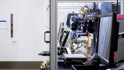
To fine-tune these inks, the crew used the Center for Nanoscale Materials (CNM) at Argonne, to look at how nanoparticles clump collectively, see how they modify with warmth and test the steadiness and make-up of the dried movies — insights that helped enhance the ink formulations. They additionally used the 2-ID-E exhausting X-ray microprobe at Argonne’s Advanced Photon Source (APS), to map the form and elemental make-up of the printed gadgets, complementing excessive‑decision X-ray spectroscopy research at Brookhaven’s National Synchrotron Light Source II (NSLS-II). CNM, APS and NSLS-II are all DOE Office of Science person amenities.
A key ingredient in these printed gadgets is vanadium dioxide. This materials is particular as a result of it will probably act like a wire, letting electrical energy move, or like an insulator, blocking electrical energy. This switching capability is vital for making electronic circuits and reminiscence gadgets, which retailer and course of info.
To management the move of electrical energy within the transistors, the crew used a course of referred to as redox gating. In easy phrases, this implies they use a chemical response so as to add or take away electrons from the vanadium dioxide. By making use of a small voltage — lower than what’s utilized in a typical battery — they’ll flip the transistor on or off. This methodology is much less harsh than different methods, which might harm the fabric and make gadgets put on out shortly.
In laboratory assessments, the printed transistors operated at voltages as little as 0.4 to 0.5 volts and stored working for greater than 6,000 on-off cycles, which is for much longer than earlier printed gadgets. The switches additionally responded shortly, altering states in about one second.
“We chose printing methods for two main reasons,” mentioned Argonne Materials Scientist Yuepeng Zhang. “First, printing enables rapid prototyping and iterative design, which helps us optimize materials and device structures quickly. Second, printed electronics have benefits for device functionality, especially since our devices show a well-modulated current response to voltage, making them suitable for printed logic devices and niche applications.”
When the printed transistor was switched on utilizing a small management sign of 0.5 volts, it allowed about 50% extra electrical energy to move by way of it in comparison with when it was off. In different phrases, the system might increase the move of electrical present by half with only a tiny quantity of energy. This exhibits that the transistor can reliably management electrical energy utilizing little or no power, which is vital for making low-power and versatile electronic gadgets.
Wei Chen, a chemist from Argonne and the University of Chicago, emphasised the sturdiness of the brand new gadgets. “Redox gating is robust and does not damage the materials, so we can run thousands of cycles without issues,” he mentioned. “In previous methods, devices could only run a few times — sometimes just 10 cycles — before failing. Our devices can run thousands of cycles with no problem.”
Right now, these printed transistors are bigger and slower than the tiny silicon chips present in most electronics. But this analysis exhibits that it’s doable to make sturdy, low-power gadgets with printing strategies.
Chen added, “From my perspective, the next step is logic devices. We’ve been in contact with industry partners interested in testing our devices for logic applications, which are the basic building blocks for computers. That is something I would like to pursue.”
They are additionally exploring how these printed gadgets may very well be utilized in neuromorphic computing, an space that mimics the way in which the human mind processes info.
To transfer printed electronics from the lab to actual merchandise, the researchers say extra teamwork is required between scientists and business. They additionally consider that artificial intelligence and machine learning might assist enhance the printing course of and make growth quicker.
“Printing involves many variables to adjust, and machine learning can help us find the best settings more quickly,” Zhang mentioned.
With extra analysis and collaboration, printed hybrid electronics might assist make future know-how extra versatile, reasonably priced and power environment friendly.
The outcomes of this analysis had been revealed in Advanced Materials Technology.
Other contributors to this work embody Samuel Miller and Hua Zhou from Argonne; and Evan Musterman, Andrew Kiss and Yang Yang from the National Synchrotron Light Source II at DOE’s Brookhaven National Laboratory. Andrew Erwin and Shiyu Hu had been at Argonne when this analysis is performed.
This work was primarily supported by the Laboratory Directed Research and Development program at Argonne, with extra assist from DOE’s Office of Science, Basic Energy Sciences.
About Argonne’s Center for Nanoscale Materials
The Center for Nanoscale Materials is among the 5 DOE Nanoscale Science Research Centers, premier nationwide person amenities for interdisciplinary analysis on the nanoscale supported by the DOE Office of Science. Together the NSRCs comprise a collection of complementary amenities that present researchers with state-of-the-art capabilities to manufacture, course of, characterize and mannequin nanoscale supplies, and represent the most important infrastructure funding of the National Nanotechnology Initiative. The NSRCs are positioned at DOE’s Argonne, Brookhaven, Lawrence Berkeley, Oak Ridge, Sandia and Los Alamos National Laboratories. For extra details about the DOE NSRCs, please go to https://science.osti.gov/User-Facilities/User-Facilities-at-a-Glance.
About the Advanced Photon Source
The U. S. Department of Energy Office of Science’s Advanced Photon Source (APS) at Argonne National Laboratory is among the world’s best X-ray mild supply amenities. The APS offers high-brightness X-ray beams to a various neighborhood of researchers in supplies science, chemistry, condensed matter physics, the life and environmental sciences, and utilized analysis. These X-rays are ideally suited for explorations of supplies and organic constructions; elemental distribution; chemical, magnetic, electronic states; and a variety of technologically vital engineering techniques from batteries to gas injector sprays, all of that are the foundations of our nation’s financial, technological, and bodily well-being. Each yr, greater than 5,000 researchers use the APS to supply over 2,000 publications detailing impactful discoveries, and resolve extra important organic protein constructions than customers of every other X-ray mild supply analysis facility. APS scientists and engineers innovate know-how that’s on the coronary heart of advancing accelerator and light-source operations. This consists of the insertion gadgets that produce extreme-brightness X-rays prized by researchers, lenses that focus the X-rays down to some nanometers, instrumentation that maximizes the way in which the X-rays work together with samples being studied, and software program that gathers and manages the huge amount of information ensuing from discovery analysis on the APS.
This analysis used sources of the Advanced Photon Source, a U.S. DOE Office of Science User Facility operated for the DOE Office of Science by Argonne National Laboratory below Contract No. DE-AC02-06CH11357.
Argonne National Laboratory seeks options to urgent nationwide issues in science and know-how by conducting modern primary and utilized analysis in just about each scientific self-discipline. Argonne is managed by UChicago Argonne, LLC for the U.S. Department of Energy’s Office of Science.
The U.S. Department of Energy’s Office of Science is the one largest supporter of primary analysis within the bodily sciences within the United States and is working to handle among the most urgent challenges of our time. For extra info, go to https://energy.gov/science.