
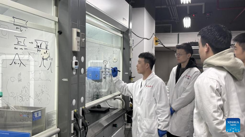
Zhang Shuchen (1st L), a member of a global research team, is pictured at a lab on the University of Science and Technology of China in Hefei, east China’s Anhui Province, Jan. 14, 2026. (University of Science and Technology of China/Handout by way of Xinhua)
HEFEI, Jan. 15 (Xinhua) — An worldwide research team has developed a “self-etching” technique to course of comfortable and unstable ionic crystal lattice semiconductors, particularly 2D perovskite thin-layer single crystals, with out damaging their construction, thereby overcoming a key problem within the subject of optoelectronic supplies.
The research, led by researchers from the University of Science and Technology of China, Purdue University and ShanghaiTech University, was revealed on Thursday within the journal Nature.
The team launched a guided “self-etching” method that leverages inside stress gathered throughout crystal development. By utilizing a gentle ligand-isopropyl alcohol (IPA) answer system, the researchers induced managed in-plane self-etching at particular websites in 2D perovskite single crystals.
Subsequently, they exactly crammed the etched cavities with 2D perovskites of various halogen compositions. This allowed the creation of high-quality heterojunctions inside a single crystal wafer, that includes lattice continuity and atomically easy interfaces.
In semiconductor optoelectronics, heterojunctions — interfaces shaped between supplies of various chemical compositions on the atomic degree — enable exact management over the optical properties of every cavity. By tuning the halogens in these etched areas, researchers can design pixel-like models with adjustable emission coloration and brightness, a vital step towards miniaturized and environment friendly optoelectronic gadgets.
Compared to standard strategies corresponding to robust solvent remedy or ultraviolet patterning, this new technique is gentler and preserves the crystal lattice from injury.
“This processing method suggests that in the future, we may integrate densely arranged microscopic light-emitting pixels of different colors on an ultra-thin material. It opens up a new material platform and design pathway for high-performance luminescent and display devices,” stated Zhang Shuchen, a member of the research team. ■