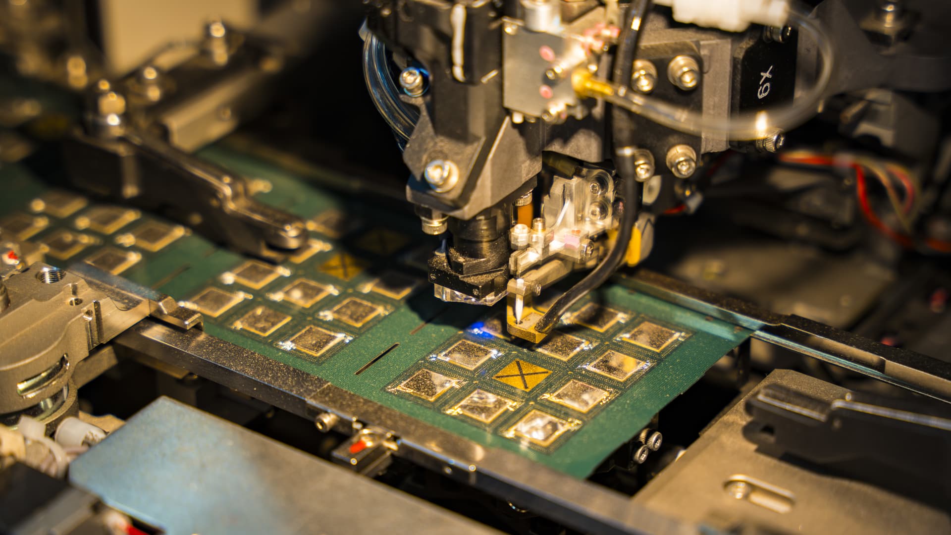
A robotic machine manufactures a semiconductor chip at a stall to present traders throughout The Advantage Assam 2.0 Investment Summit in Guwahati, India, on Feb. 25, 2025.
Nurphoto | Nurphoto | Getty Images
India desires to turn out to be a world chip main, however the odds are steep: competitors is fierce, and India is a late entrant within the race to take advantage of superior chips.
In 2022, when the U.S. restricted exports of its superior AI chips to China to curb Beijing’s entry to cutting-edge expertise, a world race for semiconductor self-reliance started.
For India, it provided a possibility: the nation desires to scale back dependence on imports, safe chips for strategic sectors, and seize a larger share of the worldwide electronics market shifting away from China.
India is one of many world’s largest customers of electronics, however it has no native chip business and performs a minimal position within the world provide chain. New Delhi’s “Semiconductor Mission” goals to change that.
The ambition is daring. It desires to create a full provide chain — from design to fabrication, testing and packaging — on Indian soil.
As of this month, the nation has authorised 10 semiconductor tasks with whole funding of 1.6 trillion rupees ($18.2 billion). These embody two semiconductor fabrication vegetation, and a number of testing and packing factories.
India additionally has a pool of engineering expertise that is already employed by world chip design firms.
Yet progress to this point has been uneven, and neither the investments nor expertise pool is sufficient to make India’s chip ambitions a actuality, say specialists.
“India needs more than a few fabs or ATP facilities (i.e., more than a few “shiny objects.”) It needs a dynamic and deep and long-term ecosystem,” stated Stephen Ezell, vp for world innovation coverage at the Information Technology and Innovation Foundation, a science and expertise coverage assume tank.
Ezell says that main semiconductor producers contemplate “as many as 500 discrete factors” earlier than they arrange multi-billion-dollar fab investments. These embody expertise, tax, commerce, expertise insurance policies, labor charges and legal guidelines and customs insurance policies — all areas the place India has work to do.
New Delhi’s coverage push
In May, the Indian authorities added a new ingredient to its chip ambition: a scheme to help digital part manufacturing, addressing a vital bottleneck.
Until now, chipmakers had no native demand for his or her product as there are hardly any digital part manufacturing firms, comparable to telephone digital camera firms, in India.
Researchers contained in the semiconductor fabrication lab on the Centre for Nano Science and Engineering, on the Indian Institute of Science, in Bangalore.
Manjunath Kiran | Afp | Getty Images
But the brand new coverage provides monetary help to firms producing lively and passive digital parts, creating a potential home buyer-supplier base that chip producers can plug into.
In 2022, the nation additionally pivoted from its technique of offering superior incentives to fabrication models making chips of 28nm or much less. When it comes to chips, the smaller the dimensions, the upper the efficiency with improved power effectivity. These chips can be utilized in new applied sciences like superior AI and quantum computing by packing extra transistors into the identical house.
But this method wasn’t serving to India develop its nascent semiconductor business, so New Delhi now covers 50% of the challenge prices of all fabrication models, no matter chip measurement, and of chip testing and packing models.
Fab firms from Taiwan and the U.Ok., and semiconductor packaging firms from the U.S. and South Korea have all proven curiosity in aiding India’s semiconductor ambitions.
“The Indian government has doled out generous incentives to attract semiconductor manufacturers to India,” stated Ezell, however he confused that “those sorts of investments aren’t sustainable forever.”
The lengthy highway
The largest chip challenge in India presently is the 910-billion-rupee ($11 billion) semiconductor fabrication plant being inbuilt Prime Minister Narendra Modi’s house state of Gujarat by Tata Electronics, in partnership with Taiwan’s Powerchip Semiconductor Manufacturing Corp.
The unit will make chips for energy administration built-in circuits, show drivers, microcontrollers and high-performance computing logic, Tata Electronics said, which can be utilized in AI, automotive, computing and information storage industries.
The U.Ok.’s Clas-SiC Wafer Fab has additionally tied up with India’s SiCSem to arrange the nation’s first business compound fab within the japanese state of Odisha.
These compound semiconductors can be utilized in missiles, defence gear, electrical automobiles, shopper home equipment and solar energy inverters, in accordance to a authorities press launch.
“The coming 3-4 years is pivotal for advancing India’s semiconductor goals,” stated Sujay Shetty, managing director of semiconductor at PwC India.
Establishing operational silicon fabrication services and overcoming technical and infrastructural hurdles that reach past incentives might be a key milestone, in accordance to Shetty.
Opportunities past fab
Fabrication websites want to meet stringent necessities, comparable to being in areas free from floods and vibrations, with dependable highway connectivity — which might current ongoing logistical concerns for some areas.
India additionally wants specialty chemical suppliers that meet “ultra-high purity standards essential for advanced semiconductor manufacturing,” Shetty added.
Beyond chip fabrication vegetation, many medium-sized firms in India have proven curiosity in establishing chip testing and packaging models. Several Indian teams are additionally coming into the section, attracted by its increased margins and decrease capital depth in contrast to fabs.
“Outsourced semiconductor assembly and testing (OSAT) represents a significant opportunity for India, though clarifying market access and demand channels will be important for sustained growth,” says Shetty.
Success on this space will see India enter the worldwide chip business, however New Delhi is nonetheless a good distance from regionally growing and manufacturing the cutting-edge of chip expertise: 2nm semiconductors.
These 2nm chips supply higher efficiency and energy effectivity due to their smaller transistor measurement. Taiwan Semiconductor Manufacturing Corporation will begin mass-producing cutting-edge 2nm chips later this 12 months, according to an FT report.
NEW DELHI, INDIA – MAY 14: Union Minister of Railways, Information and Broadcasting, Electronics and Information Technology Ashwini Vaishnaw briefing the media on Cabinet selections at National Media Centre on May 14, 2025 in New Delhi, India.
Hindustan Times | Hindustan Times | Getty Images
Last week, Indian minister Ashwini Vaishnaw, who was in Bengaluru to inaugurate a new workplace of semiconductor design agency ARM, stated the British firm will design the “most advanced chips used in AI servers, drones, mobile phone chips of 2 nm” from the south Indian metropolis.
But specialists say the position of native expertise is possible to be restricted to non-core design testing and validation, because the core mental property for chip designs is typically held in places just like the U.S. or Singapore, the place established IP regimes help such actions.
“India has sufficient talent in design space, because unlike semiconductor manufacturing and testing that has come up in the last 2 years, design has been there since 1990s,” stated Jayanth BR, a recruiter with over 15 years of expertise in hiring for world semiconductor firms in India.
He stated world firms often outsource “block-level” design validation work to India.
Going past this is one thing India’s authorities will want to resolve if it desires to fulfil its semiconductor ambitions.
“India may consider updating its IP laws to address new forms of IP, like digital content and software. Of course, improving enforcement mechanisms will go a long way in protecting IP rights,” says Sajai Singh, a accomplice at Mumbai-based JSA Advocates & Solicitors.
“Our competition is with countries like the U.S., Europe, and Taiwan, which not only have strong IP laws, but also a more established ecosystem for chip design.”