The program is designed to introduce excessive school college students to the semiconductor trade through genuine, hands-on laboratory expertise.
Unlike most excessive school STEM enrichment programs, ATLAS locations college students inside an lively analysis fabrication facility. Over two weeks, individuals full virtual reality coursework, security coaching and hands-on actions inside CNF’s 17,000-square-foot cleanroom, one of the superior college nanofabrication amenities within the nation. Before heading to the lab, college students take CNF’s three-day virtual Technology and Characterization at the Nanoscale curriculum, which supplies the scientific basis for what they later create.
“Having this kind of access is transformative,” mentioned David Syracuse, the teacher with New Visions Engineering. “It shows students that science and engineering are more than a lab report you write after a 45-minute experiment. They get to see the full story – from an idea to the work it takes to develop it, to sharing results – and understand that engineering is always a collaborative effort.”
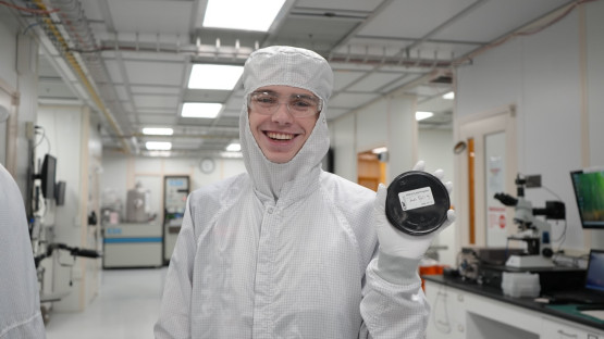
Once cleared for cleanroom entry, college students go well with up in specialised clothes and enter CNF’s fabrication bays, the place college researchers and visiting scientists routinely construct microscale and nanoscale units. Staff display how chips start as naked, single-crystal silicon wafers and introduce college students to the instruments and processes used to layer, sample, and etch the tiny circuits that energy fashionable electronics.
“One of my favorite parts of the ATLAS program was seeing how so many different disciplines can make discoveries and advancements with nanotechnology. We learned from people researching everything from cancer detection to solar efficiency to quantum computing devices. The experience encouraged me to approach problems holistically and collaborate across disciplines to find solutions,” mentioned Iris Johnson, New Visions Engineering scholar.
For most college students within the group, it was the primary time seeing how the {hardware} inside on a regular basis units is bodily manufactured.
Building the semiconductor workforce pipeline
ATLAS is gaining renewed relevance at a pivotal second for New York State’s semiconductor sector. On Jan. 16, Micron Technology broke floor on its $100 billionmegafab advanced in Onondaga County –the most important personal funding within the historical past of the state, described by federal officers as one of many largest industrial tasks in U.S. historical past. The growth is anticipated to generate tens of 1000’s of technical jobs, with Micron estimating 9,000 direct hires and 50,000 whole jobs created not solely in fabrication but additionally throughout a community of suppliers, coaching courses and analysis establishments.
“The construction of the Micron Technology megafab will change the shape of the state’s economy for decades to come,” mentioned Thomas Pennell, CNF’s Workforce Development Program Manager and ATLAS lead teacher. “Current estimates are that by the year 2030 over 25% of the chips manufactured in the United States will be made on the I-90 corridor,”
Pennell defined how ATLAS is already serving to place college students to benefit from that development. “Since we launched it in 2023, nine students have returned to CNF for National Science Foundation (NSF)-funded Research Experiences for Undergraduates and internships supported by the Northeast Regional Defense Technology Hub (NORDTECH),” he mentioned. “We’re seeing students shift their trajectories toward high-tech industries.”
Inspiring the following era of chipmakers
For the excessive school college students who participated, the cleanroom expertise was greater than a tour; it was a glimpse of what it means to work on the forefront of contemporary know-how, and their first encounter with a quickly increasing trade.
“As a programmer, working in a cleanroom made me more familiar with the processes leading up to the code running on the silicon. I think this experience will help greatly with future software engineering,” mentioned Clayton Melson, New Visions Engineering scholar.
“My time in the clean room has certainly impacted my decision for my intended field of study. Initially, when going into the cleanroom, I had determined my major to be biomedical engineering. After my time in the clean room, and the discovery of how microfluidic devices aid in the research of microbiology, I was able to whittle my interest in biomedical engineering to a nano-specific biological approach,” mentioned Niveck VonBergen, New Visions Engineering scholar.
Syracuse expanded on how early publicity to skilled semiconductor environments helps college students join classroom studying to real-world careers whereas growing transferable expertise. “This type of experience shows students that professional skills matter just as much as technical knowledge,” he mentioned. “Being able to communicate clearly, work on a team and show up prepared are skills they can carry into college or any career.”
“By experiencing the ATLAS program and developing my own personal wafer, I gained a newfound interest in nanotechnology,” mentioned Ari Wessell, New Visions Engineering scholar. “I really hope to work in a cleanroom facility in the future, and I’m interested in the endless possibilities in the world of nanotechnology.”