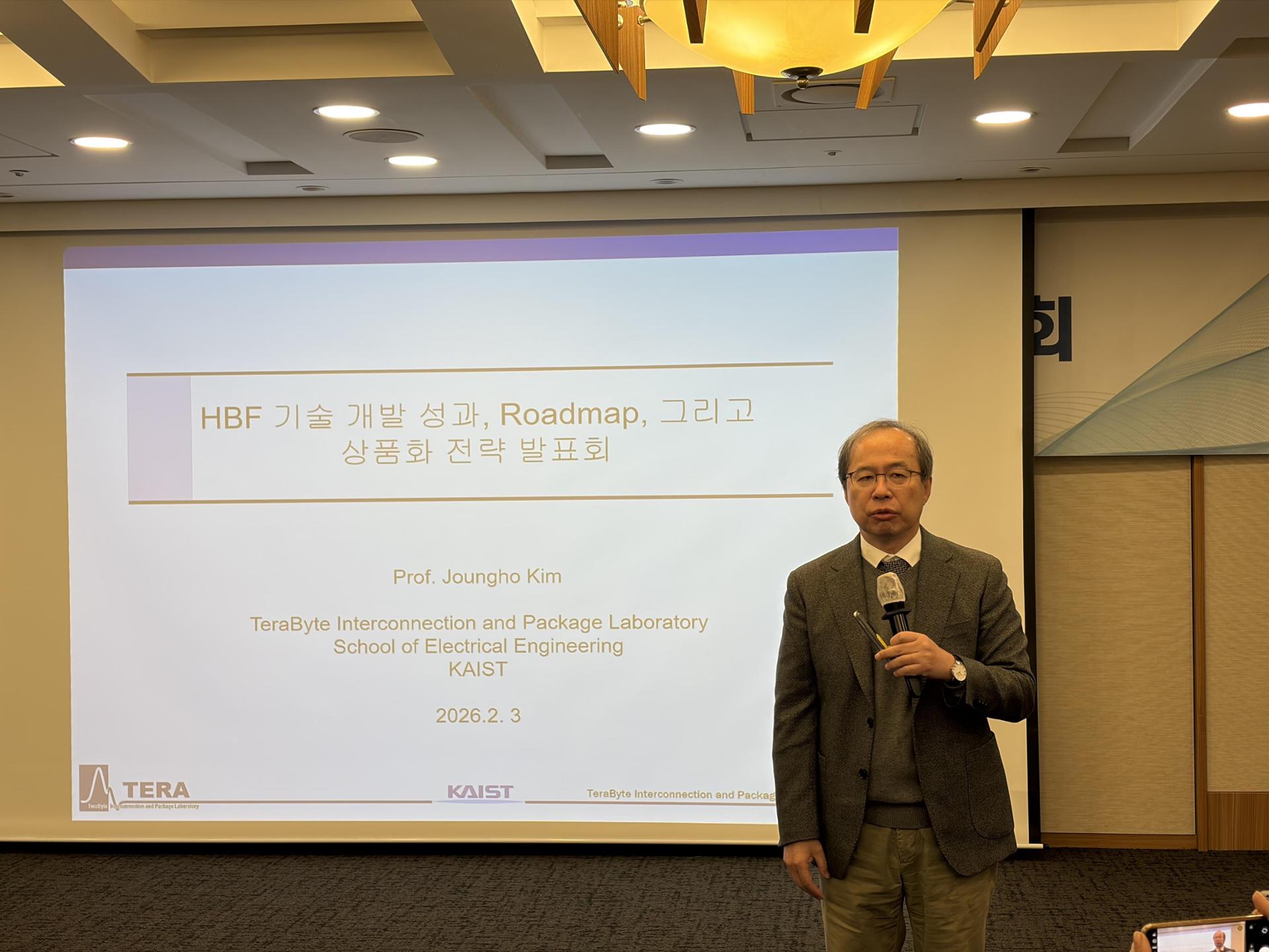
Professor Kim Joung-ho of the Korea Advanced Institute of Science and Technology speaks throughout a press convention on high-bandwidth flash on the Korea Press Center in Seoul, Tuesday. Korea Times picture by Nam Hyun-woo
Professor Kim Joung-ho of the Korea Advanced Institute of Science and Technology (KAIST), recognized for devising the fundamental construction of high-bandwidth reminiscence (HBM), launched a road map for high-bandwidth flash (HBF), a next-generation chip structure for high-performance storage that will probably be vital for synthetic intelligence (AI) inference.
“So far, graphics processing units (GPUs) have played a central role in AI computing, but going forward, memory will become even more important than GPUs,” Kim stated throughout a press convention in Seoul on Tuesday.
“After years of research, HBM has been commercialized successfully and is now driving the AI era. With HBF, we aim to make another leap forward and lead the AI era through memory-centric computing.”
Memory, principally dynamic random-access reminiscence (DRAM) chips, serves as a quick, short-term and unstable workspace for lively information and functions. Storage, largely based mostly on NAND flash, features as a non-volatile repository, retaining recordsdata and apps at bigger capability however slower speeds.
The significance of NAND flash has been rising quickly in AI accelerators, as AI companies more and more shift towards inference, which requires quick and frequent entry to giant volumes of saved information to ship real-time outcomes.
While HBM is manufactured by vertically stacking DRAM chips, HBF is a brand new resolution that vertically stacks NAND flash to keep up solid-state-drive-level capability whereas aiming to attain bandwidth growth corresponding to HBM. To allow this, applied sciences utilized in HBM manufacturing will probably be required.
A diagram displaying a graphics processing unit subsequent to high-bandwidth reminiscence and high-bandwidth flash chips / Courtesy of KAIST Tera Lab
Kim proposed a construction wherein HBF could be positioned alongside the GPU and HBM, thereby permitting HBM to work as “a bookshelf near the GPU” and HBF “a library near the GPU.”
“In the PC era, Intel led the global market as CPU was the key component, while in the smartphone era, Qualcomm took the lead as power efficiency became critical,” he stated. “In the AI era, memory will be the key determinant, with HBM driving speed and HBF defining capacity.”
Kim stated HBF might be commercialized in late 2027 or early 2028, noting that design and course of experience collected by HBM improvement has considerably shortened the trail to commercialization. He added that Samsung Electronics and SK hynix are working with Nvidia, Google, AMD and different main tech corporations to roll out HBF-powered chips inside that time-frame.
“Companies need HBM capabilities to develop HBF as well,” he stated. “Since Samsung Electronics and SK hynix possess technologies in both areas, their market dominance is expected to strengthen further compared to other memory companies. Going forward, it will become a hegemony game in which GPUs cannot operate without memory.”
Kim’s lab, KAIST Tera Lab, is called a breeding floor for semiconductor consultants. Around 40 Tera Lab alumni work at home reminiscence giants together with Samsung Electronics and SK hynix, whereas one other 40 or so are employed at main U.S. tech corporations resembling Apple.
KAIST Tera Lab will maintain a web-based Zoom presentation session on HBF expertise improvement, workload evaluation and its road map at 9 a.m. Feb. 10. A recording of the livestream will probably be accessible on the lab’s web site (http://tera.kaist.ac.kr).