By Che Pan and Laurie Chen
BEIJING, March 5 (Reuters) – Top Chinese semiconductor executives have referred to as for a coordinated nationwide effort to develop operational lithography programs throughout the 2026-2030 interval, underlining Beijing’s push for larger technological self-reliance.
Zhao Jinrong, chairman of Naura Technology Group, Chen Nanxiang, chairman and president of Yangtze Memory Technologies Corp, and Liu Weiping, chairman of Empyrean Technology, co-authored an article alongside main semiconductor institutes that was revealed on-line late on Wednesday.
They urged the federal government to pool nationwide sources to combine technological breakthroughs throughout establishments.
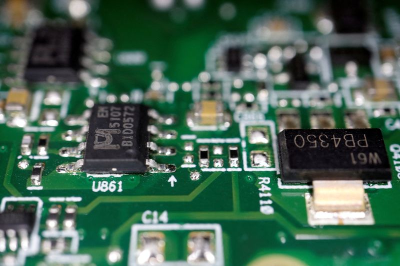
Semiconductor manufacturing has emerged as a crucial battleground within the China-U.S. know-how rivalry since 2020, with Washington actively imposing restrictions to cease China from increasing superior manufacturing capability beneath 7-nanometer.
“Taking lithography machines as an example, ASML’s extreme ultraviolet (EUV) equipment has 100,000 components supplied by 5,000 suppliers, with ASML merely serving as the integrator,” the executives wrote in Science and Technology Review, a journal affiliated with China’s science and know-how professionals affiliation.
Dutch agency ASML Holding has develop into the world’s sole provider of EUV lithography machines, important for producing probably the most superior semiconductor chips used to energy smartphones, AI and superior computing.
“How to establish China’s ASML, so that the ‘integrated’ can jump out of the barrier of ‘fame and fortune’, and uniformly allocate funds and human resources is an urgent issue that relevant departments should immediately formulate implementation plans,” they wrote.
SEMICONDUCTOR AND NATIONAL STRATEGY
China has made breakthrough progress at totally different establishments in EUV laser gentle sources, wafer stage, and optical programs, however integrating these parts into a whole system stays a problem that should be solved throughout the fifteenth five-year plan interval, they stated.
The article additionally recognized bottlenecks in digital design automation (EDA) software program, supplies corresponding to silicon wafers and digital gases as key areas requiring national-level coordination.
China designated semiconductors as a core pillar of its nascent trade alongside aviation, biotechnology and the low-altitude economic system in its newest authorities work report launched on Thursday.
Chinese Premier Li Qiang highlighted breakthroughs in domestically pushed chip analysis and growth efforts throughout the report.
The five-year roadmap made no particular point out of lithography machines, calling as a substitute to ‘improve advanced process manufacturing capabilities, accelerate the development of key equipment, materials and components.
China’s chip manufacturing capability on the mature 28nm node and above accounts for 33% of worldwide capability and stays unrestricted in each manufacturing and design, in accordance to an article revealed in Science and Technology Review.
In the identical article, the executives additionally referred to as for establishing public platforms with probably the most superior course of capabilities to analysis, develop and confirm the most recent gadget constructions, course of gear, parts, supplies and EDA software program.
(Reporting by Che Pan and Laurie Chen; Editing by Jacqueline Wong)