The course of would surpass typical lithography machines, that are the principle manner right now of creating the semiconductors used in most electronics.
When a lithography machine etches a chip circuit, the laser strikes the fabric vertically. If gentle goes sideways, it causes uncontrolled harm, significantly in comfortable supplies corresponding to lead halide perovskites.
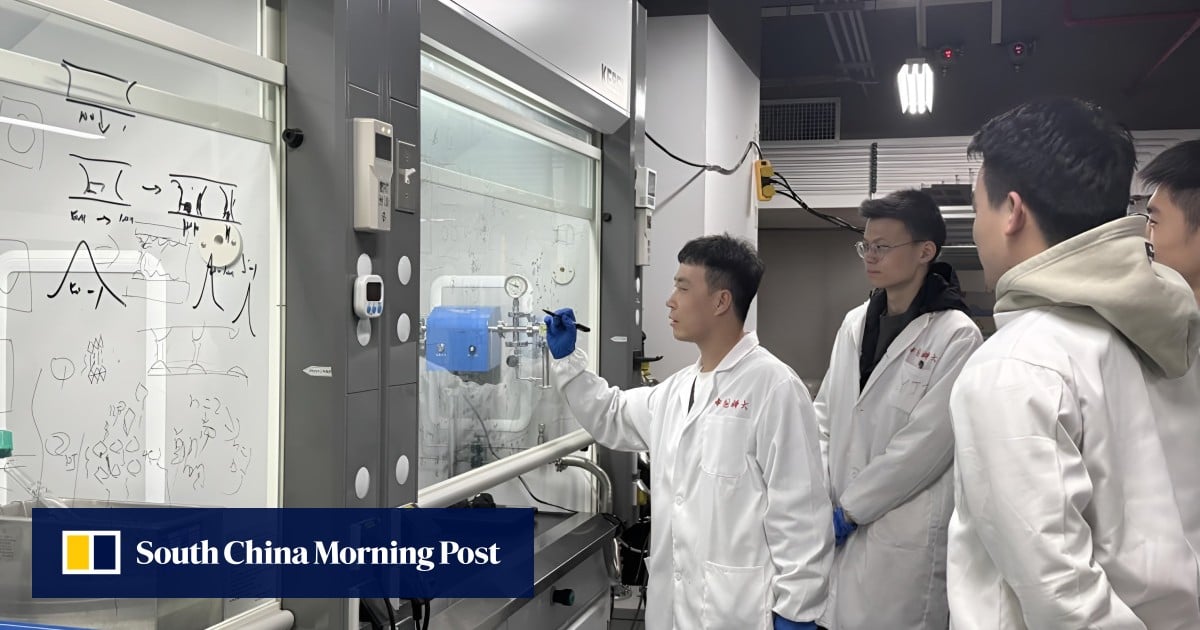
Lead halide perovskites are a really promising space of semiconductors due to their distinctive optoelectronic properties in two-dimensional crystal lattice kind however they’re troublesome to machine exactly on account of their comfortable and unstable nature in 2D.
However, the new course of creates lateral microstructures in these perovskites in a managed manner, including a new dimension that could result in revolutionary efficiency enhancements in semiconductors.
The worldwide crew stated it had developed a novel “self-etching” approach that enabled the world’s first fabrication of intricate constructions in superthin perovskite supplies with out damaging their construction.