Arizona’s rise as a semiconductor powerhouse is being acknowledged by trade leaders, who will collect in Phoenix this week for SEMICON West, the largest microelectronics trade show in North America.
SEMICON West will run Oct. 7–9 at the Phoenix Convention Center — the primary time the flagship occasion will happen outdoors of California in its 55-year historical past. The occasion will be a showcase of semiconductor developments made in Arizona and at Arizona State University.
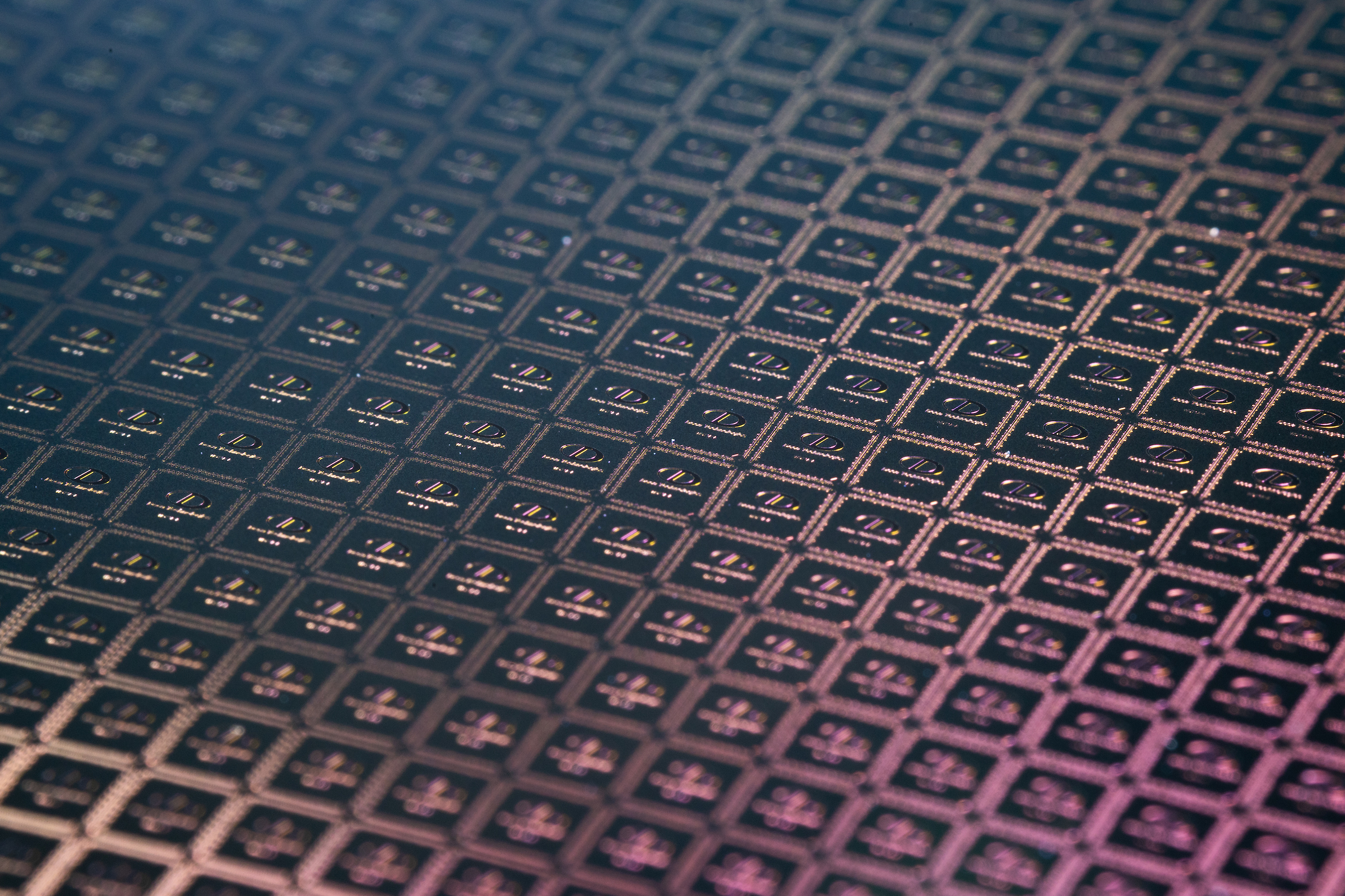
ASU, which leads a number of the largest initiatives as a part of the CHIPS and Science Act, works throughout the whole semiconductor ecosystem — from cutting-edge analysis to superior packaging, large-scale manufacturing and workforce improvement, and may have an in depth presence at SEMICON West.
ASU President Michael Crow will ship a keynote handle, and a number of other college consultants will give shows, together with Binil Starly, director of the School of Manufacturing Systems and Networks, who will talk about how AI and robots can be utilized in harmful circumstances in fabrication labs.
ASU may have an exhibit sales space designed as a central useful resource to share the college’s semiconductor analysis, business collaboration and workforce-training packages.
SEMICON West’s transfer to Phoenix is a validation of ASU’s method, in accordance to Kyle Squires, senior vice provost of engineering, computing and know-how and dean of the Ira A. Fulton Schools of Engineering.
“We have focused strategically as the university on semiconductor tech, workforce, research and development, innovation, spinouts. And it’s always good when the external community around the country and around the world is admiring what you do and learning more about us,” he stated.
“This is an opportunity for us to continue to elevate our profile. You have proximity, you have an opportunity to interact and to show examples of what we do.”
Workforce improvement is a selected focus of the conference, because the trade faces hundreds of unfilled jobs. A latest survey of firms by the SEMI Foundation, sponsor of the conference, signifies that greater than 5% of engineering positions are open as a result of U.S. universities aren’t producing sufficient graduates.
ASU engineering college students already linked with employers throughout Semiconductor Week on campus final month, and the Phoenix occasion will give them the chance to community and turn into linked to profession paths. The conference’s largest sponsor is TSMC, the corporate that’s investing billions right into a chip-manufacturing complicated in Phoenix.
“ASU is one of the largest producers of talent that is needed by the industry ecosystem, not just one particular company,” Starly stated.
“Our academic programs are aligned to produce that — not just at the bachelor’s level, but also master’s and PhD.”
Students and up to date grads in engineering, laptop science, chemistry, physics, math, knowledge science and enterprise are inspired to attend SEMICON and might get a free pass that admits them to displays, networking occasions, keynote addresses and panel discussions. There’s additionally a lounge for younger professionals and a spot without spending a dime headshots.
ASU can even show the way it’s been reaching K–12 students to spark curiosity in careers within the semiconductor trade. ASU and ASU Prep leaders will current their Okay–12 microelectronics training mannequin, which goals to attain 25,000 Okay–12 college students and 500 academics within the subsequent 5 years with exploration occasions, experiential studying and tutorial pathways for highschool.
Also, a student-created sport, Future Fab Heroes, will be launched at the Arizona Science Center, and also will be within the SEMI Foundation sales space at SEMICON West. The immersive coaching simulation, geared to center schoolers, can be downloaded and performed by anybody.
“We didn’t outsource that to professional developers — it was students developing with some staff and mentor guidance. They are video game designers and computer programmers who know nothing about microelectronics, and they’ve had to learn it,” Starly stated.
On Oct. 9, ASU and Applied Materials will mark the launch of the Materials-to-Fab Center at ASU within the Macrotechnology Works constructing situated at ASU Research Park. That $270 million lab, introduced two years in the past, will pace the switch of improvements from ideation to fab prototype.
“Applied Materials is a leader in their sector, semiconductor equipment and tools processing. And they want to have this center here because Phoenix is this hotbed of innovation talent,” Squires stated.
“Applied Materials could have put this in a lot of places, but they chose to put it here.”